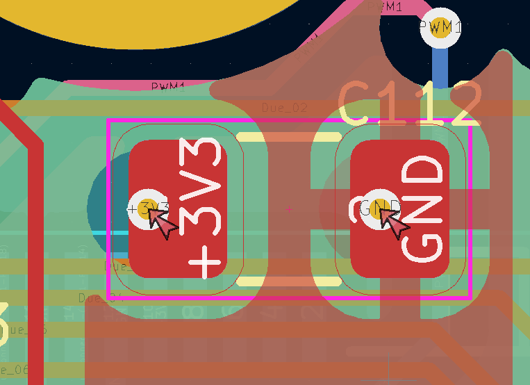
Current development builds for KiCAD 7 include the new constraint keyword physical_hole_clearance for detecting hole and pad collisions within a common net. This is useful for detecting via-in-pads which are often undesirable, as some PCB vendors upcharge to plug vias that could cause wicking during assembly.
To set up the custom design rule, first install a nightly build of KiCAD (6.99). Please note that saving a project with a development version of KiCAD will prevent older versions from opening the PCB file. To prevent this, I run the DRC from KiCAD 6.99 and make the necessary changes from KiCAD 6.
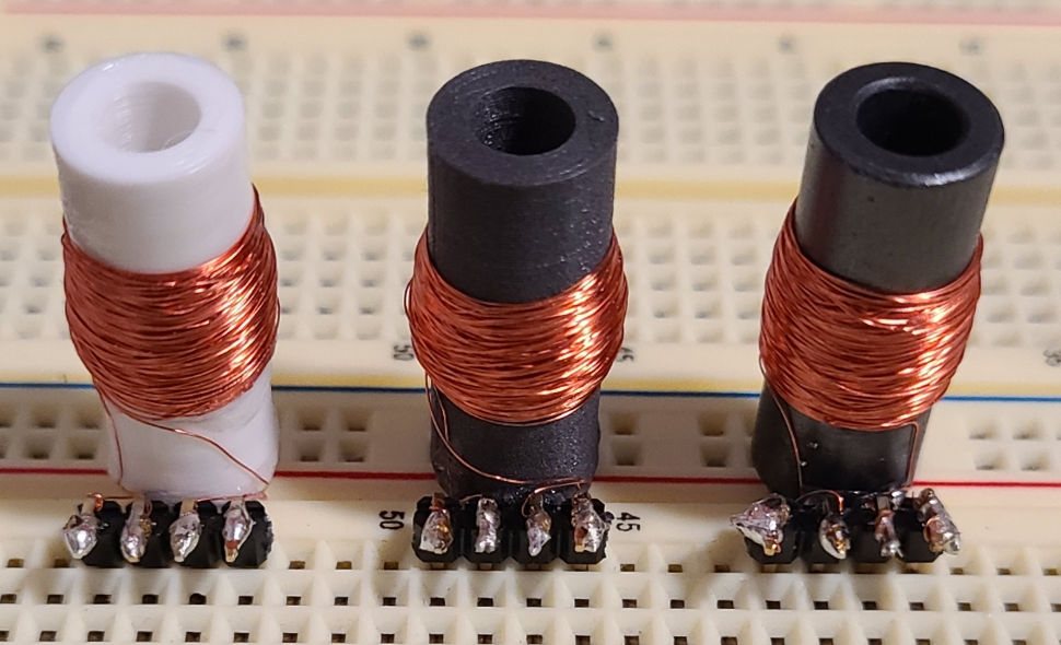
I bought a spool of Protopasta iron-filled PLA to test in a project where I need to fit a flyback transformer into a confined space. The prototype will likely be 3D-printed in PLA plastic and contain some moving parts wrapped in magnetic wire for power transfer.
For optimal performance, flyback transformers are generally wound around a ferrite core, which has high magnetic properties but low conductivity to reduce eddy currents.


