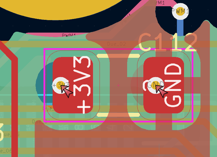
Current development builds for KiCAD 7 include the new constraint keyword physical_hole_clearance for detecting hole and pad collisions within a common net. This is useful for detecting via-in-pads which are often undesirable, as some PCB vendors upcharge to plug vias that could cause wicking during assembly.
To set up the custom design rule, first install a nightly build of KiCAD (6.99). Please note that saving a project with a development version of KiCAD will prevent older versions from opening the PCB file. To prevent this, I run the DRC from KiCAD 6.99 and make the necessary changes from KiCAD 6.
From PCB Editor, click File → Board Setup → Design Rules → Custom Rules. Then enter the following text into the text field:
(version 1)

(rule via_in_pad
    (constraint physical_hole_clearance (min 0.1mm))
    (condition "B.Pad_Type == 'SMD'"))
Now running the DRC will detect and flag any instances of vias within 0.1mm of an SMD.
